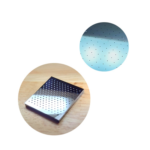
2D Fiber Array
2D Fiber Array (High-precision Hole Substrate)
TSV — Unmatched Precision, Full Customization
Built on a foundation of advanced semiconductor manufacturing processes, our via array platform delivers industry-leading precision, uniformity, and design flexibility.
Ultra-High Pitch Accuracy
Leveraging semiconductor lithography and etching processes, we achieve extremely fine pitch precision, enabling the highest density interconnects with exceptional dimensional control.Precision Wafer Bonding for Multi-Layer Integration
Our high-precision wafer bonding technology supports multi-layer stacking, meeting exact total thickness specifications while delivering excellent beam pointing angle accuracy — critical for optical alignment and beam steering applications.Lithography-Defined Aperture Control
Precise photo-lithographic control ensures tight aperture tolerances and outstanding uniformity across the entire wafer, eliminating part-to-part variation and improving system-level yield.Wafer-Level Thinning & Polishing for Via Parallelism
Dedicated wafer-level thinning and polishing processes guarantee the parallelism of through-via arrays, essential for consistent optical path length or electrical signal integrity.Customization Via Count
The number of via is fully configurable to match your specific design requirements. From prototypes to volume production, we provide the exact via count your application demands.
Trusted by industry leaders — stable, high-volume supply proven.
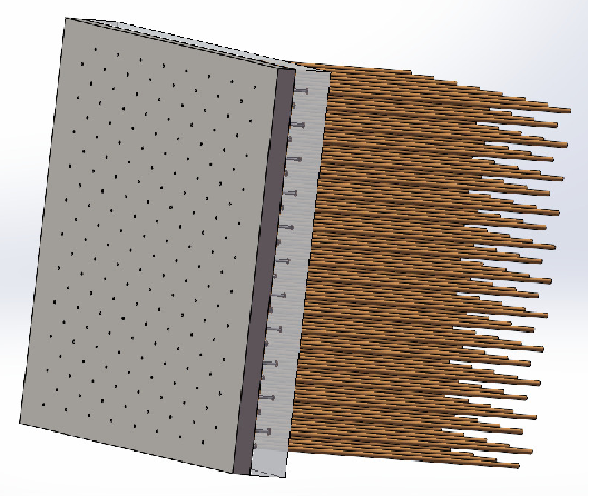
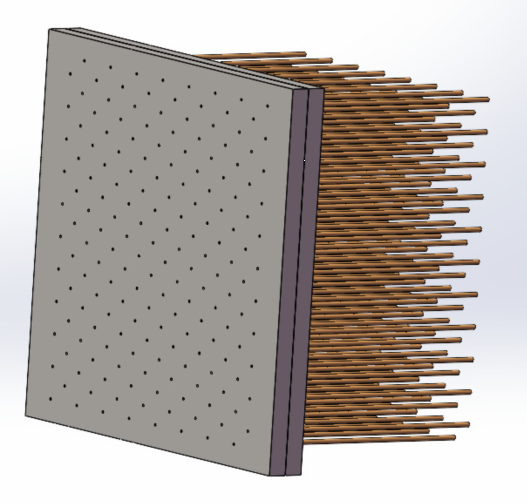
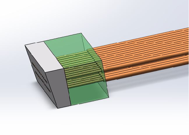
Silicon-Glass Wafer Bonding Multi-Layer Silicon Bonding 8° Angle Design